Focused-ion-beam circuit edit (FIB-CE) is a method for modifying microdevices after fabrication, by using streams of ions to either etch new features into the devices or deposit new materials. It allows engineers to do rapid prototyping to validate design changes without going through the traditional microfabrication process, saving time and money.
However, high-energy ion beams can damage existing electronic structures on a fabricated chip, and guiding them precisely requires reference points etched into the chip surface, which are used to visually align the ion beam. Etching those reference points requires the “sacrifice” of part of the chip’s surface near the region of interest.

In a pair of recent papers (paper 1 | paper 2), Amazon’s Annapurna Labs, which designs chips to the specific needs of Amazon Web Services, demonstrated that using lower-energy ion beams — 5 kiloelectronvolts (keV) instead of the standard 30 — enables the addition of new features to a fabricated chip without the need for sacrificial areas and with minimal effect on existing structures.
Moreover, lower-energy beams also enable the postproduction creation of larger features, with improved electronic characteristics, so the modified chips run more efficiently as well as using space more efficiently.
FIB-CE
FIB-CE has been around for more than two decades, and the most intuitive analogy for it is a bypass surgery: the patient is a silicon chip, and the blood vessels are metallic interconnects that need to be cut and rerouted.
The FIB microscope uses a stream of ions (usually gallium) to either image or etch features into a microdevice. If a precursor gas is injected into the microscope’s chamber, it will react with the ions to deposit insulators or conductive materials where the ion beam strikes. The experienced user can use FIB-CE to modify a microprocessor at precise locations on a nanometer scale.
Annapurna Labs designs silicon chips for AWS, which are manufactured using the world’s leading fabrication technologies, so they have extremely dense circuit layouts. This means that sacrificing part of the chip to create reference points (“fiducials”) will often destroy functional circuitry. Sometimes, it’s possible to route around the sacrificed circuitry, but sometimes it’s not.
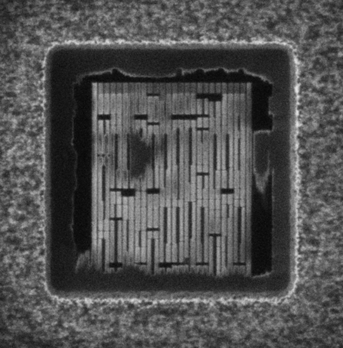
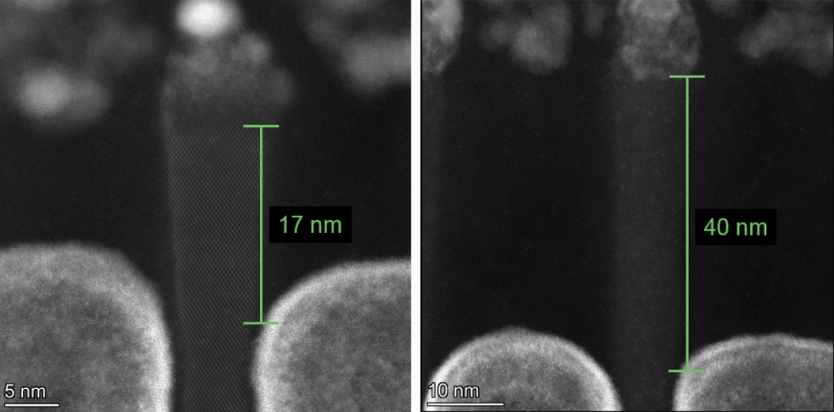
In our work, we use 5 keV ion beams to remove the bulk silicon surface layer of the chip, exposing fabricated silicon fins in the active layer beneath it. This is a standard step in most ion beam chip edits. We show that exposing even a large area has only a minor effect on the chip’s functionality.
Experiments
To test our approach, we designed a modified chip with dynamic ring oscillators (DROs) embedded in it at regular locations. A DRO consists of an odd number of inverting gates in sequence, and its output steadily oscillates between two voltage values.
After using low-energy (5 keV) FIB to create insulating trenches between oscillators, we also bathed the DROs themselves with 5 keV ion beams, to measure the effect of inadvertent exposures. Afterward, we found that they exhibited a minor shift in frequency but otherwise worked properly.

Moreover, we found that, with our method, we were able to expose larger areas around the region of interest than was possible using the higher-energy (30 keV) method, as the use of fiducials for alignment constrains the high-energy ion beam to a narrow scan width, limiting feature size.
In our experiments, we found that the larger size of our exposed area increases the number of secondary electrons arriving to the microscope’s electron detectors, thus improving the microscope’s signal-to noise ratio. This enables the FIB user to modify chip features more precisely.
Consequently, we can perform more and more-accurate FIB experiments for every chip run, enabling us to bring improved designs to our customers more cheaply and more quickly.


